7.1. Module description
Goal : Detailed explanation for each module of the processor we implemented
[Provided circuit diagram analysis and modification]
[Most important point to consider]
1. Each stage has 1 clock cycle time. (In other words, the MODULE_armreduced output pc update and pipeline registers use the same edge.)
Therefore, the 15th block of reg[31:0] registers[15:0] of MODULE_RegisterFile, which takes the role as a pc register, must be removed separately. If not implemented in this way, an error(Can't resolve multiple constant drivers for net "<name>" at <location>(ID: 10028)) will occur.
2. Considering the existence of output RD3 of MODULE_RegisterFile
3. HAZARD detection MODULE and pipeline register operation according to each signal
[Modules that have changed or added the given code]
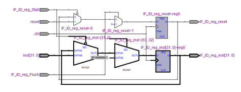
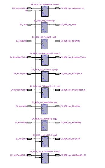
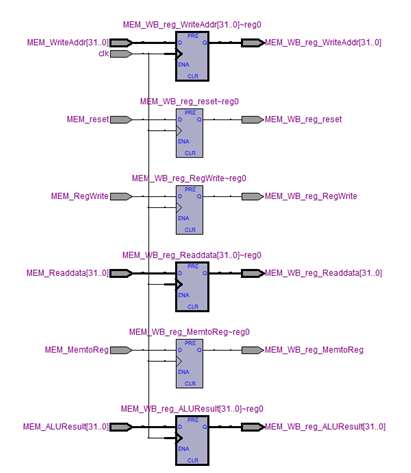
MODULE_IF_ID_reg (RTL VIWER 3. MODULE_IF_ID_reg), MODULE_ID_EX_reg (RTL VIWER 4. MODULE_ID_EX_reg), MODULE_EX_MEM_reg (RTL VIWER 5. MODULE_EX_MEM_reg), MODULE_MEM_WB_reg (RTL VIWER 6. MODULE_MEM_WB_reg) are modules that update pipeline registers in posedge.
[Hazards]
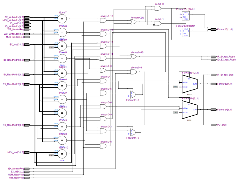
module Hazard(
input MEM_RegWrite,
input WB_RegWrite,
input EX_MemtoReg,
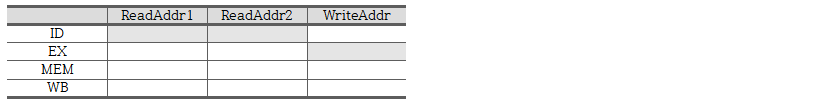
input[3:0] ID_ReadAddr1,
input[3:0] ID_ReadAddr2,
input[3:0] EX_ReadAddr1,
input[3:0] EX_ReadAddr2,
input[3:0] ID_WriteAddr,
input[3:0] EX_WriteAddr,
input[3:0] MEM_WriteAddr,
input[3:0] WB_WriteAddr,
input MEM_MemtoReg,
input WB_MemtoReg,
input EX_NZCV_Z,
input[31:0] ID_inst,
input[31:0] EX_inst, //inst[27:25] == 101 && inst[24] == 0
input[31:0] MEM_inst,
output reg[1:0] ForwardA,
output reg[1:0] ForwardB,
output reg[1:0] ForwardC,
output reg IF_ID_reg_Flush,
output reg ID_EX_reg_Flush,
output reg PC_Stall,
output reg IF_ID_reg_Stall
);- Structural hazard
We shouldn’t worry about memory lane congestion
Provided ARM processor has separate data path for instruction fetch
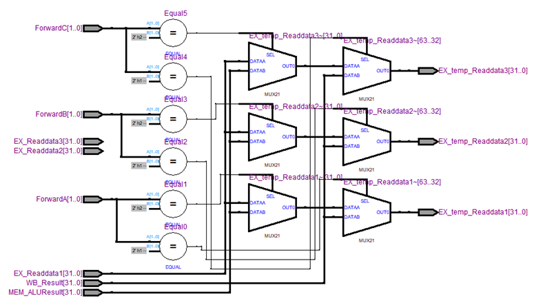
- Data hazard
We should implement data forwarding. Using unnecessary stalls will give you negative points. When a data hazard occurs by “LW” instruction, STALL is required. In this process, not only the forwarding is required, but we also need to preserve the data in this stage.
At this data hazard process, the STALL is implemented by not updating the pipeline registers.
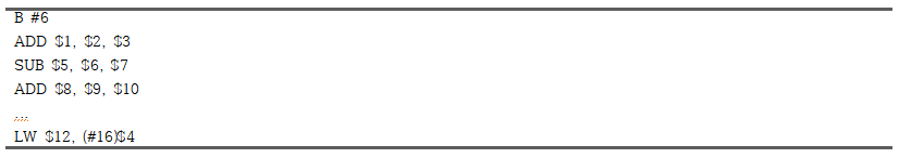
For example, lets say that the following instructions are executed:

      ForwardA <= 2'b00;
      ForwardB <= 2'b00;

      if((WB_WriteAddr == MEM_WriteAddr) && (MEM_WriteAddr == EX_ReadAddr1) && (MEM_RegWrite == 1'b1)) begin
         ForwardA <= 2'b10;
      end
      if((WB_WriteAddr == MEM_WriteAddr) && (MEM_WriteAddr == EX_ReadAddr2) && (MEM_RegWrite == 1'b1)) begin
         ForwardB <= 2'b10;
      end
      if((WB_WriteAddr == EX_ReadAddr1) && (WB_RegWrite == 1'b1)) begin
         ForwardA <= 2'b01;
      end
      if((WB_WriteAddr == EX_ReadAddr2) && (WB_RegWrite == 1'b1)) begin
         ForwardB <= 2'b01;
      end
      if((MEM_WriteAddr == EX_ReadAddr1) && (MEM_RegWrite == 1'b1)) begin
         ForwardA <= 2'b10;
      end
      if((MEM_WriteAddr == EX_ReadAddr2) && (MEM_RegWrite == 1'b1)) begin
         ForwardB <= 2'b10;
      end
      if((MEM_WriteAddr == EX_WriteAddr) && (MEM_RegWrite == 1'b1)) begin
         ForwardC <= 2'b01;
      end
      if((WB_WriteAddr == EX_WriteAddr) && (WB_RegWrite == 1'b1)) begin
         ForwardC <= 2'b10;
      end
      PC_Stall <= 1'b0;

      IF_ID_reg_Stall <= 1'b0;
      ID_EX_reg_Flush <= 1'b0;


      if(((ID_ReadAddr1 == EX_WriteAddr) || (ID_ReadAddr2 == EX_WriteAddr)) && (EX_MemtoReg == 1'b1) ) begin //LW
         PC_Stall <= 1'b1;
         IF_ID_reg_Stall <= 1'b1;
         ID_EX_reg_Flush <= 1'b1;
      end
- Control hazard
We can use stalls(pc) for branch and NOP.
For this example, what we need to flush is the two ADD instructions and one SUB instruction.

      IF_ID_reg_Flush <= 1'b0;
      ID_EX_reg_Flush <= 1'b0;

      if(((EX_NZCV_Z == 1'b1) && (EX_inst[27:25] == 3'b101) && (EX_inst[24] == 1'b1)) || ((MEM_inst[27:25] == 3'b101) && (MEM_inst[24] == 1'b0))) begin
         IF_ID_reg_Flush <= 1'b1;
         ID_EX_reg_Flush <= 1'b1
As we can see from the chart above, when there are extra instructions right after conditional instruction, there must be a bubble, in order to execute the instruction, which corresponds to the targeted pc. The reason why there are three bubbles is, the pipeline register in between ID stage and EX stage will be flushed.
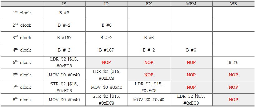

As we can see from the result of our Time Simulation, this is the way how the instruction flow working on. Due to the result of the Branch Instruction, the instruction address will be affected and so it will not flow sequentially anymore. As a solution, we use STALL. At this point, we will use FLUSH method, in order to replace the instructions that have entered before we decide to take the instruction corresponds to the result of the target PC address by (B #6) branch instruction.
Since at the 4th clock, the MEM_inst[27:25] equals to 3’b101 and MEM_inst[24] equals to 1’b0, both of IF_ID_reg_Flush and ID_EX_reg_Flush will be assigned the value of 1’b1. This will be resulted into the flush, which is equal to completely resetting and filling the blank with bubbles.
7.2. Timing Simulation
[Timing Simulation]
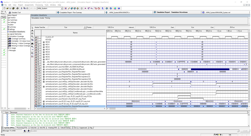
[Analysis of results and failure factors]
As we can see from the Time Simulation image, we failed to reach to the loop statement.
By adding some important nodes to the Time Simulation, we analyzed the causes of our error by following 3 reasons:
First, the possibility of asynchronous between Pipeline Register Update Clock and Register File Update Clock. At CIRCUIT DIAGRAM 3. modified 5-stage pipelined processor, we defined the Pipeline Register Update as ‘posedge’, but after our re-analysation, we found out that it is more natural for Pipeline Register Update to be ‘nededge’.
Second, the possibility of incomplete implementation whilst separating PCregister. As we can see from [CIRCUIT DIAGRAM 3. modified 5-stage pipelined processor], we figured out that the 15th index of the Register File has to be separated with PCregister, in order for pc to be moved out as an output whenever it wants to be. We tried to implement this instruction as a verily code, but maybe due to our insufficient understanding of verilog, it might result into incorrect operation.

Third, the consideration of edge used by the modules we did not implement by ourself. We suffered lack of understanding of the overall operation of the program because we failed to analysis the modules that we are using inside of arm-reduced module and testvec.s.
'학부공부 > Logic Design & Computer Architecture' 카테고리의 다른 글
| 8. ARM 5stage pipeline report 2 [Computer Architecture] (0) | 2021.12.02 |
|---|---|
| 6. ARM instruction 분석 report [Computer Architecture] (0) | 2021.12.02 |
| 3. Project 3_Calculator [Logic Design] (0) | 2021.12.02 |
| 2. Project 2_Missionaries and cannibals problem [Logic Design] (0) | 2021.12.02 |
| 1. Project 1_Missionaries and cannibals problem [Logic Design] (0) | 2021.12.01 |


댓글